

A Partly TurnKey PCBA service optimizes costs by executing a collaborative hybrid model: your engineering team retains control over specialized, highly proprietary components while Shenzhen Hongda Circuit Technology Co., Ltd. (PCBKR) manages the PCB fabrication, standard SMT components (passives and standard ICs), stencil engineering, and final automated assembly
Why Is the Partly TurnKey Hybrid Model Winning the 2026 Hardware Market?
As we navigate the 2026 hardware landscape, architectural demands have hit a literal physical wall
A standard circuit board trace at 56 GHz (the Nyquist frequency of 224G PAM4) acts less like a passive trace and more like an inefficient antenna
Partly TurnKey Hybrid Operational Model
| Responsibility Domain | Core Components & Managed Processes | Operational Value |
|
Customer Domain (Consigned) |
Proprietary ASICsHigh-Cost FPGAsSpecialized Sensors |
Secured directly by Customer to avoid markup and verify origin |
| (Transfer) |
Components securely shipped to assembly lines |
Eliminates procurement overhead |
|
PCBKR Domain (Turnkey Sourcing & Mfg) |
High-Speed Low-Loss Material Procurement (Megtron 8/M9/Ultra-Low Df)Ultra-HDI PCB Fabrication (mSAP, Any-layer HDI, Blind/Buried Vias)Commercial-Off-The-Shelf (COTS) BOM Sourcing (Resistors, Caps, LDOs)Precision SMT Assembly & Advanced Inspection (SPI, 3D AOI, X-Ray) |
Single-source responsibility for fabrication yields and assembly precision |
1. Advanced 2026 PCB Fabrication Technology Integration
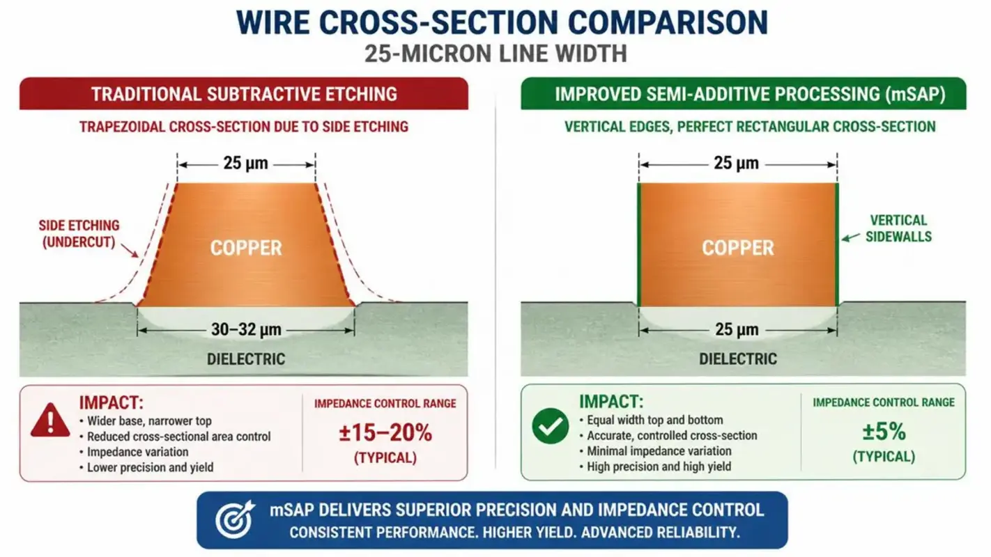
Wire Cross-Section Comparison at 25-Micron Line Width (Subtractive Etching vs. mSAP)
At Shenzhen Hongda Circuit Technology Co., Ltd., we have updated our manufacturing lines to process next-generation substrates
-
Material Matrix Control: We build multi-layer stacks using ultra-low-loss resin systems (such as Panasonic Megtron 8 or Doosan M9) blended with PPO/hydrocarbon hybrid resins
. These materials sustain a Df as low as 0.0012 to 0.0015 to stop signal attenuation . -
Copper Profile Optimization: We deploy Hyper-Very-Low-Profile (HVLP) copper foils with an inner-layer surface profile roughness (Rz) less than 1.0 micron, reducing the severe high-frequency skin effect losses that occur at 56 GHz
. -
mSAP (Modified Semi-Additive Process): To support compact, high-density designs, our mSAP technology allows trace width and spacing to scale down to 25 microns / 25 microns, abandoning the traditional subtractive etching limitations (75 microns) and maintaining precise impedance tolerances of plus or minus 5%
.
2. Resolving Critical Substrate & Assembly Manufacturing Pain Points
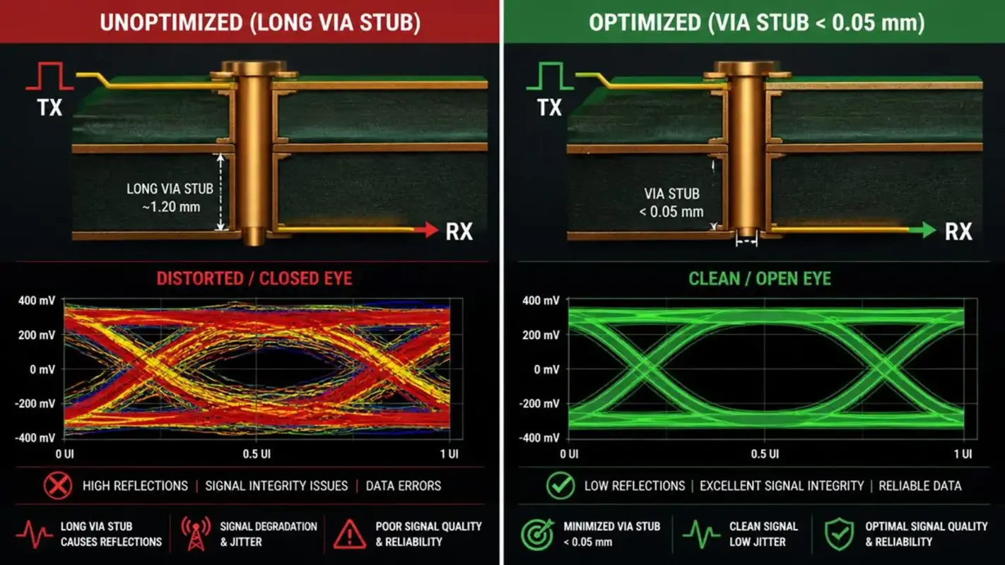
Impact of Controlled-Depth Backdrilling on Via Stub and Signal Eye Diagram
Managing a purely consigned model or a full turnkey model for ultra-high-speed AI server boards often results in steep cost penalties due to structural pain points
The Via Stub Resonance Trap
In high-speed multilayer boards, any un-etched vertical via stub behaves as a resonant open circuit
-
Our Engineering Solution: We execute computer-controlled, depth-controlled backdrilling to reduce residual stubs to less than 0.05 mm (2 mils), removing the resonant copper residue entirely
.
Glass Weave Effect Jitter
Standard E-glass fabrics have unequal dielectric distributions between the fiberglass bundles and the resin gaps
-
Our Engineering Solution: We mandatorily deploy mechanically spread 1067 or 1078 Ultra-Spread Flat Glass Fabrics to ensure a uniform dielectric constant (Dk) landscape across the entire substrate
.
3. Technical Parameter Comparison Matrix
The table below contrasts our technical execution across partial turnkey assembly setups for standard commercial versus ultra-high-speed hardware
| Technical Parameter | Standard Commercial PCBA Target | High-Speed AI/Server PCBA Target (2026) |
| Layer Count Capabilities |
4 to 8 Layers |
16 to 32+ Layers Rigid Backplane |
| Substrate Core Material |
Standard FR4 (Tg 150 degrees Celsius) |
Ultra-Low Loss Hydrocarbon/PPO (Tg greater than 180 degrees Celsius) |
| Minimum Trace / Spacing |
75 microns / 75 microns |
25 microns / 25 microns (via mSAP Line Definition) |
| Dielectric Loss Tangent (Df) |
0.015 to 0.020 at 1 GHz |
0.0012 to 0.0015 at 28 GHz / 56 GHz |
| Impedance Tolerance Control |
Plus or minus 10% Standard |
Plus or minus 5% Rigorous (TDR Verified) |
| Via Structure Engineering |
Through-hole via structures |
Laser-drilled Stacked Microvias (Any-Layer HDI) |
| Residual Via Stub Target |
N/A |
Less than 0.05 mm (2 mils) via Controlled Backdrilling |
| Component Placement Pitch |
0.4 mm pitch ICs / 0402 passives |
0.35 mm to 0.3 mm pitch FBGA / 01005 passives |
Frequently Asked Questions (FAQ)
How does Shenzhen Hongda Circuit Technology Co., Ltd. prevent component mix-ups in a Partly Turnkey scenario? We execute an electronic incoming material verification workflow
Which components should we consign, and which should we let PCBKR source? You should consign highly specialized ICs, proprietary microcontrollers, custom ASICs, and long-lead components where you maintain direct distributor allocation priorities
How does backdrilling impact the overall fabrication cost of my high-speed boards? Backdrilling adds a specialized, computer-controlled secondary drilling run to remove unused via copper stubs
What structural data is required from our design team to ensure accurate mSAP execution? To process mSAP trace generation down to 25 microns, your design files must include net-specific single-ended or differential impedance targets (e.g., 50 Ohm/100 Ohm), reference plane allocations, and exact material designation preferences
How are assembly defects managed if a customer-consigned component is found faulty? Every assembly undergoes 3D Automated Optical Inspection (AOI) and 3D X-Ray (AXI) testing to confirm mechanical placement alignment, soldering integrity, and voiding percentages (controlled strictly to less than 15%)