Guide to Low-Temperature Co-fired Ceramic (LTCC) PCB Specifications for Advanced Electronics Manufacturing
Low-Temperature Co-fired Ceramic (LTCC) technology is a cornerstone of modern high-performance electronics, enabling the creation of robust, multi-layered circuits for demanding applications in aerospace, telecommunications, and medical devices. Understanding the fundamental manufacturing specifications of LTCC PCBs is critical for successful design and integration. This article outlines the key technical parameters that define the capabilities of standard LTCC processes.
Key Geometrical and Electrical Specifications
The performance of an LTCC substrate is largely determined by its physical dimensions and conductor properties. The following specifications form the baseline for design:
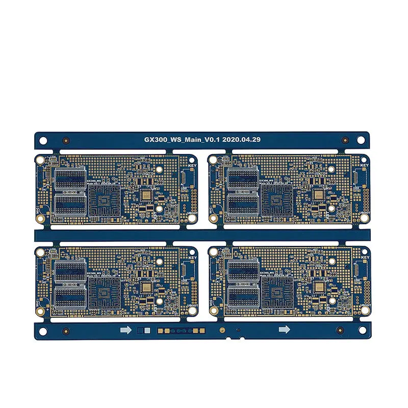
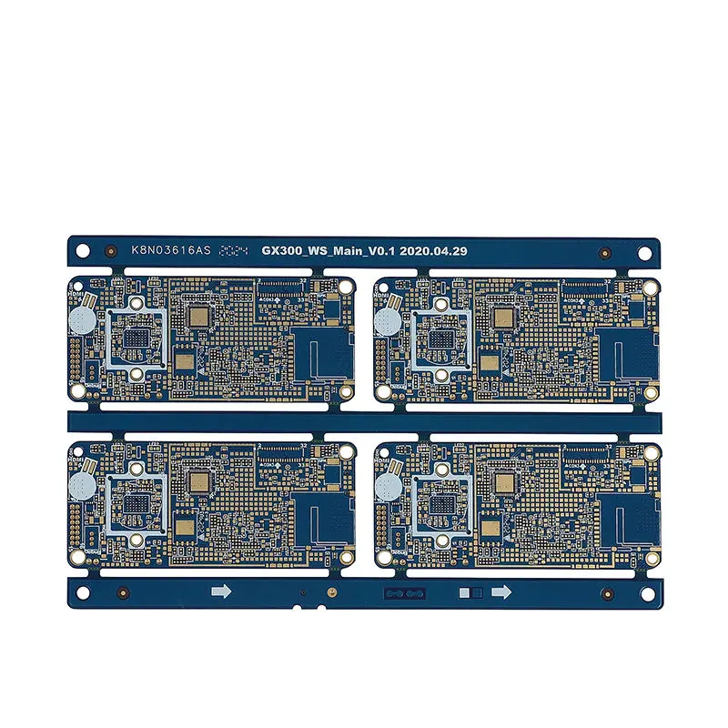
1、Maximum Substrate Size: The standard panel size is limited to 100 mm x 100 mm, which is optimal for housing multiple compact modules or a single, complex circuit.
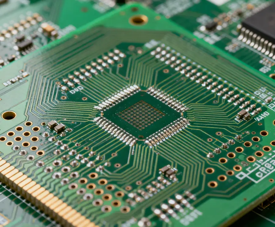
2、Fine-Line Printing Capability: Achieving high circuit density is possible with a minimum line width and spacing of 0.075 mm and 0.15 mm respectively. The printing line width accuracy is maintained within ±10 μm, ensuring consistent electrical characteristics across the board.
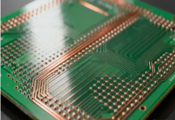
3、Conductor Thickness: The printed conductor thickness typically ranges from 10 to 25 μm, providing a balance between current-carrying capacity and fine-feature resolution.
Critical Registration and Dimensional Tolerances
Precision in layer alignment and dimensional stability during the high-temperature sintering process is what sets LTCC apart. These tolerances are vital for reliable multi-layer interconnect:
1、Layer-to-Layer Alignment: The stack alignment accuracy is ≤ 30 μm, guaranteeing precise registration between all layers for reliable via connections.
2、Sintering Control: LTCC technology excels in its predictable shrinkage, with a sintering shrinkage accuracy of ±0.2%. This allows designers to accurately predict the final dimensions of the fired substrate.
3、Micro-Via Formation: The process supports the creation of micro-vias with a minimum through-hole diameter of 0.1 mm, enabling high-density vertical interconnects.
Design Rule Checks (DRC) for Optimal Yield
Adhering to minimum spacing rules is essential for manufacturing yield and long-term reliability. Key design rules include:
1、Edge Clearance: A minimum distance of 0.2 mm between conductors and the substrate edge is required to prevent chipping or cracking.
2、Via-to-Line Spacing: The distance between a metal through-hole and a conductor line must be at least 0.15 mm to ensure electrical isolation.
3、Integrated Passive Components: The technology allows for the direct printing of resistors. The minimum overlap distance for a resistor and its conductor is 0.15 mm, and the minimum resistor size is 0.15 mm x 0.15 mm.
Multi-Layer Capability
LTCC technology supports highly complex, integrated subsystems by allowing a significant number of layers. The maximum total number of dielectric layers can be up to 40, providing ample room for intricate signal, power, and ground planes in a single, hermetic package.
The specifications outlined above demonstrate the high-precision capabilities of LTCC PCB manufacturing. Mastery of these parameters—from fine-line geometry and tight tolerances to extensive multi-layer support—enables engineers to push the boundaries of miniaturization and performance. When designing for LTCC, close collaboration with your manufacturing partner to leverage these specifications is the key to unlocking the full potential of this advanced ceramic technology.
Maximum substrate size: 100 mm × 100 mm
Minimum line width / spacing: 0.075 mm / 0.15 mm
Conductor thickness (printed): 10–25 μm
Printing line width accuracy: ±10 μm
Stack alignment accuracy: ≤30 μm
Minimum through-hole diameter: 0.1 mm
Sintering shrinkage accuracy: ±0.2%
Minimum conductor-to-edge clearance: 0.2 mm
Minimum via-to-line distance: 0.15 mm
Minimum resistor/conductor overlap: 0.15 mm
Minimum resistor dimensions: 0.15 mm × 0.15 mm
Maximum number of dielectric layers: 40 layers
 PCB Key Specifications")